V Nand Vs 3d Nand
3d nand is a new powerful entry into the ssd conversation.
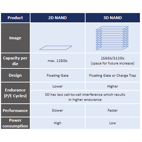
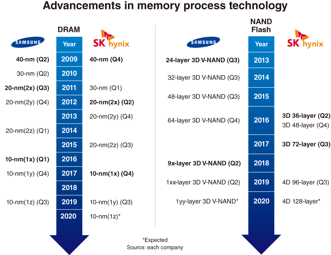
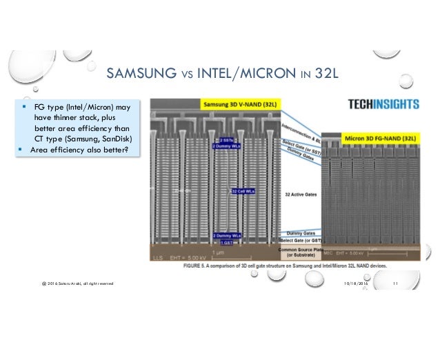
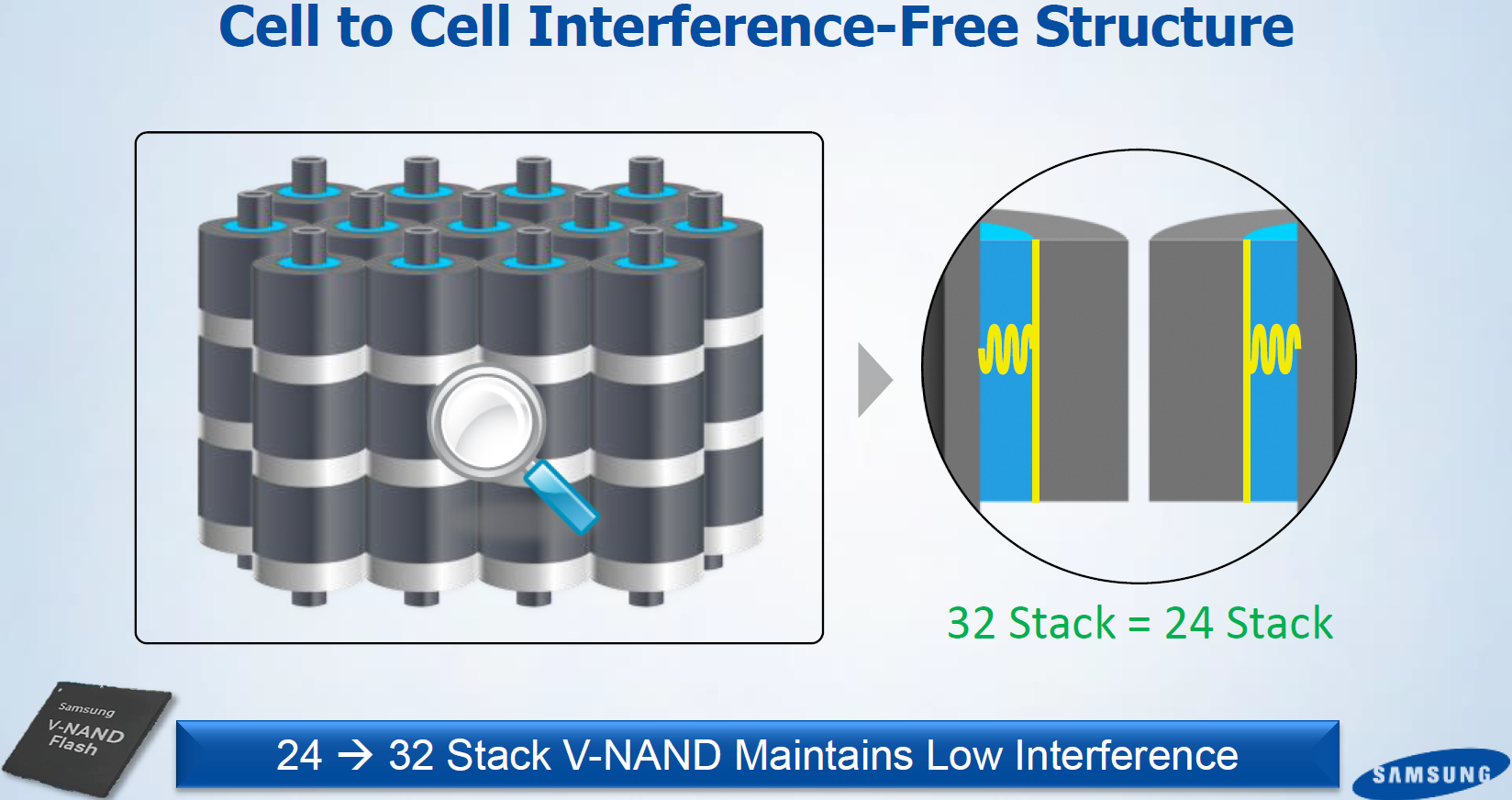
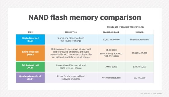
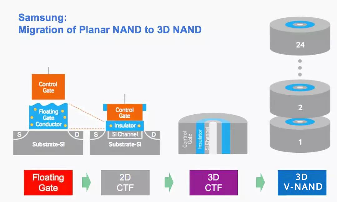
V nand vs 3d nand. Samsung lays claim to the v nand name with the difference usually being in the fact that their stacks are even more stacked than before such as 48 layers where there were once 32 meaning of course more capacity once again. This is where planar nand single planes of nand cells are stacked vertically giving the v in v nand. The difference is in propriety. Nand has better endurance than nor reportedly up to 10 times and faster write and erase speeds thanks to the way data is organised in blocks.
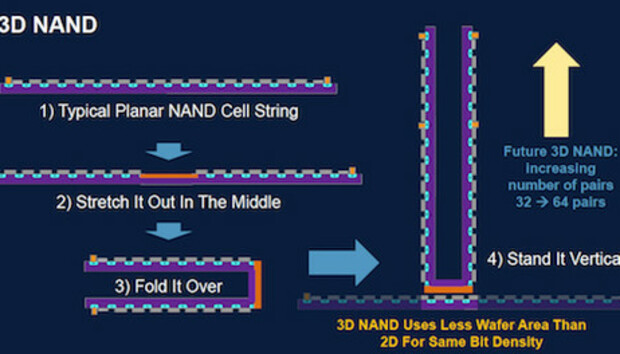
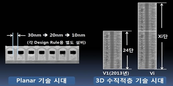
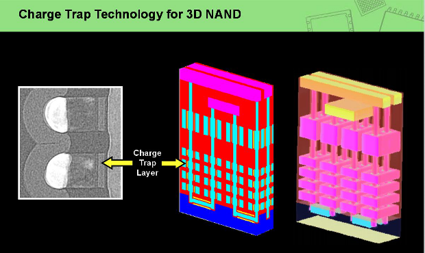
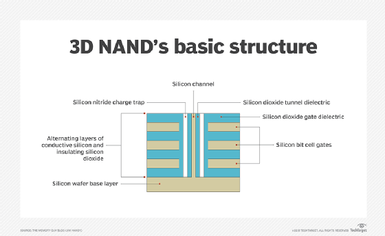
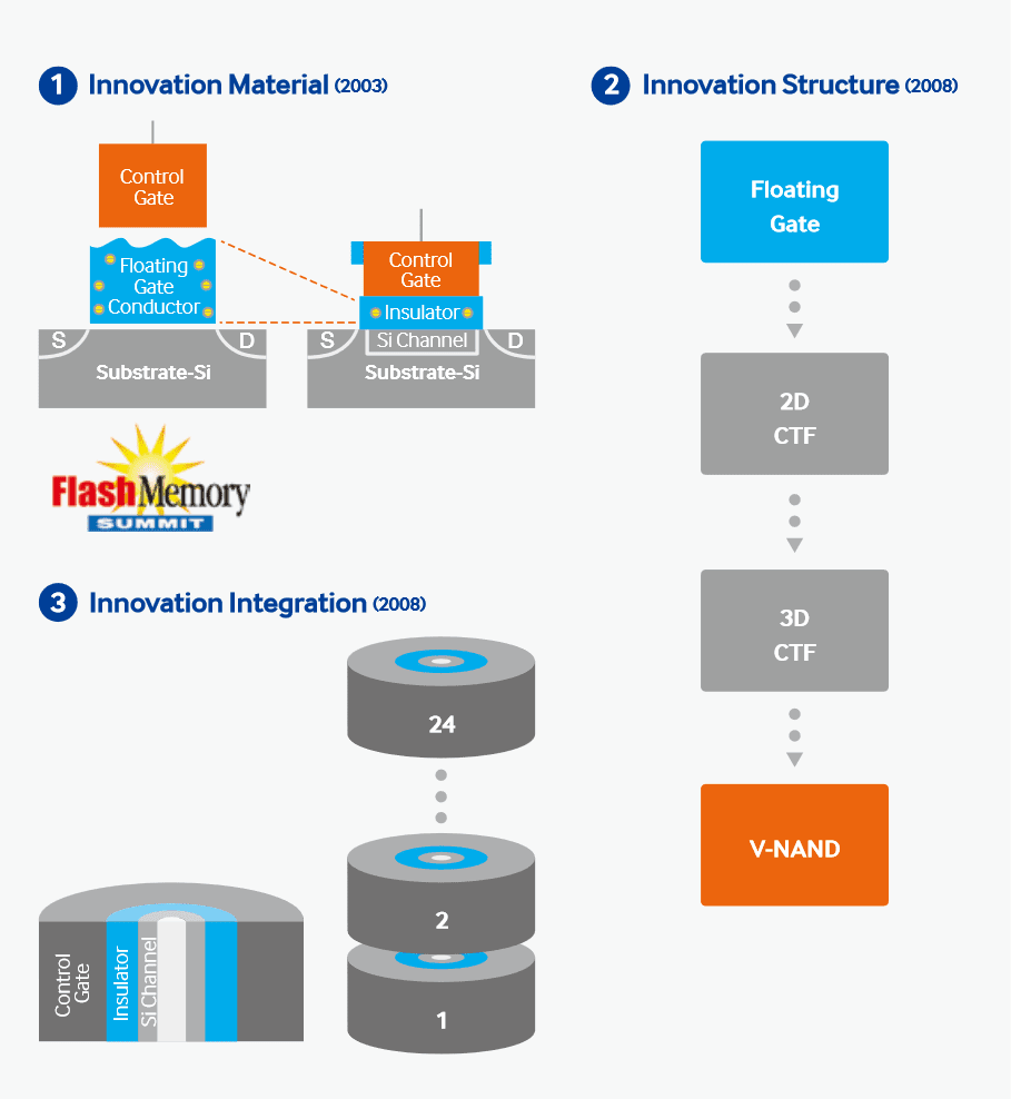
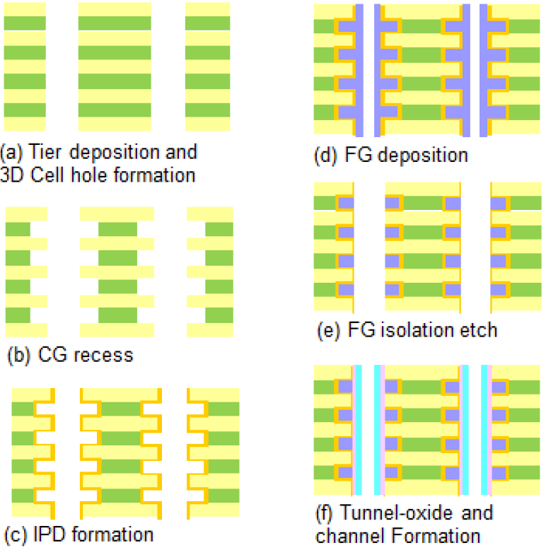
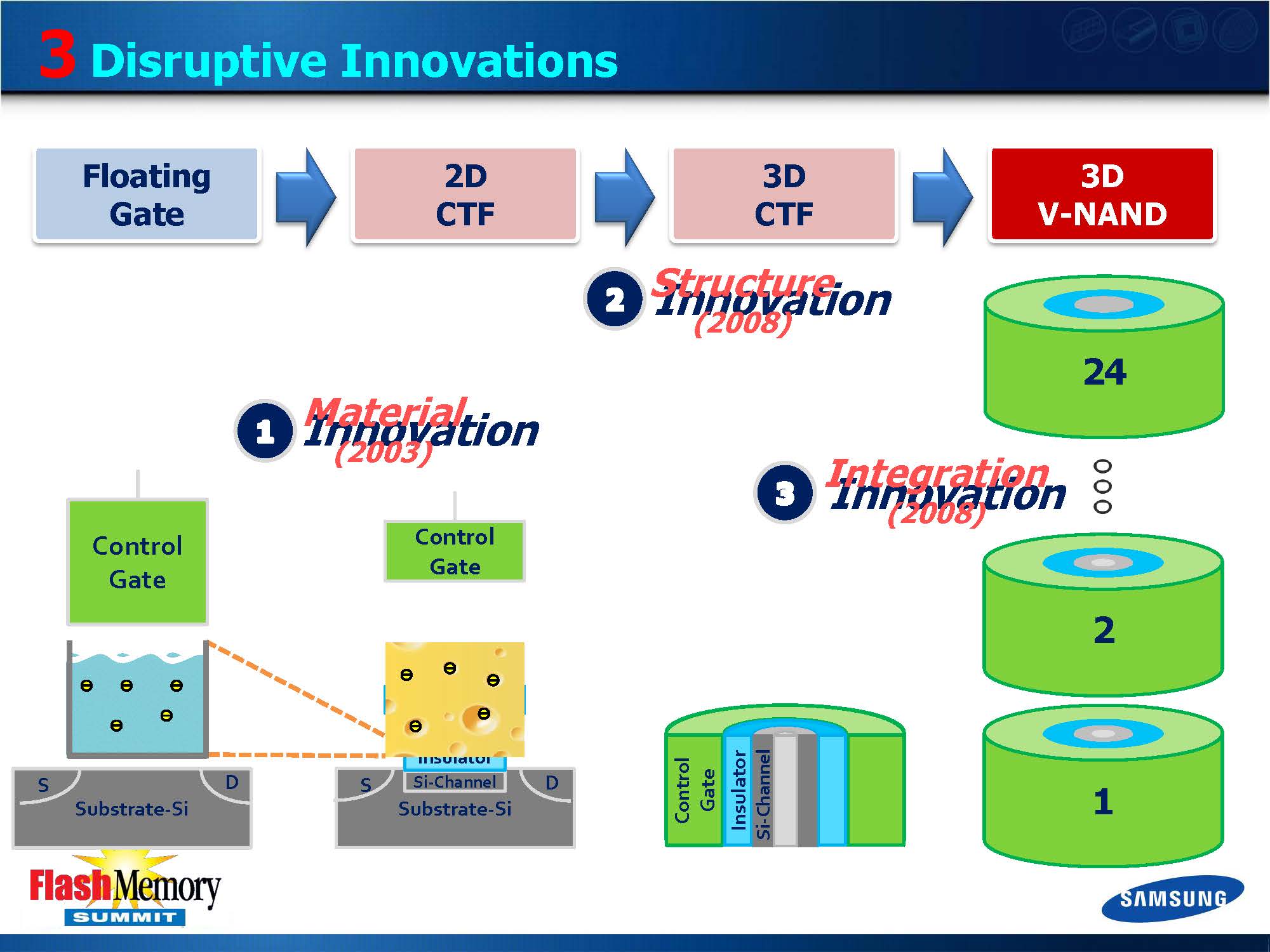
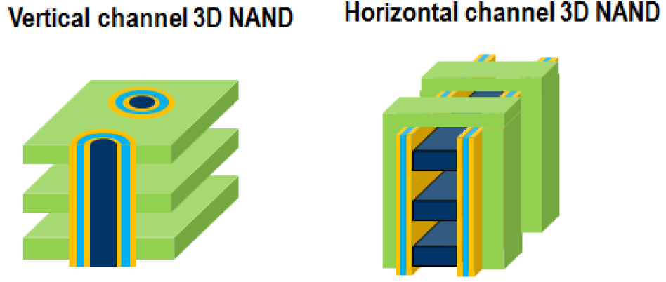
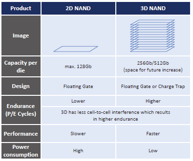
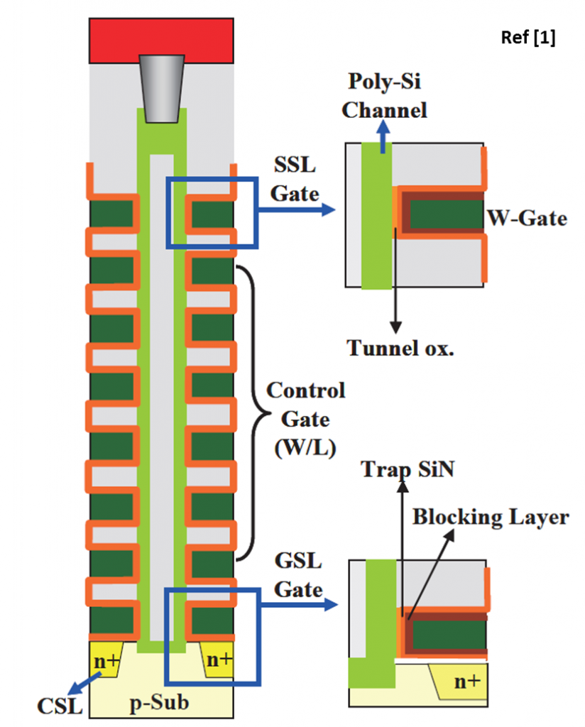
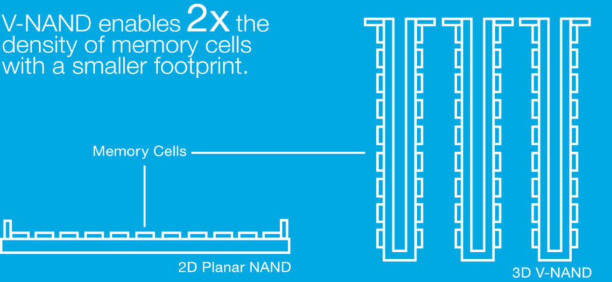
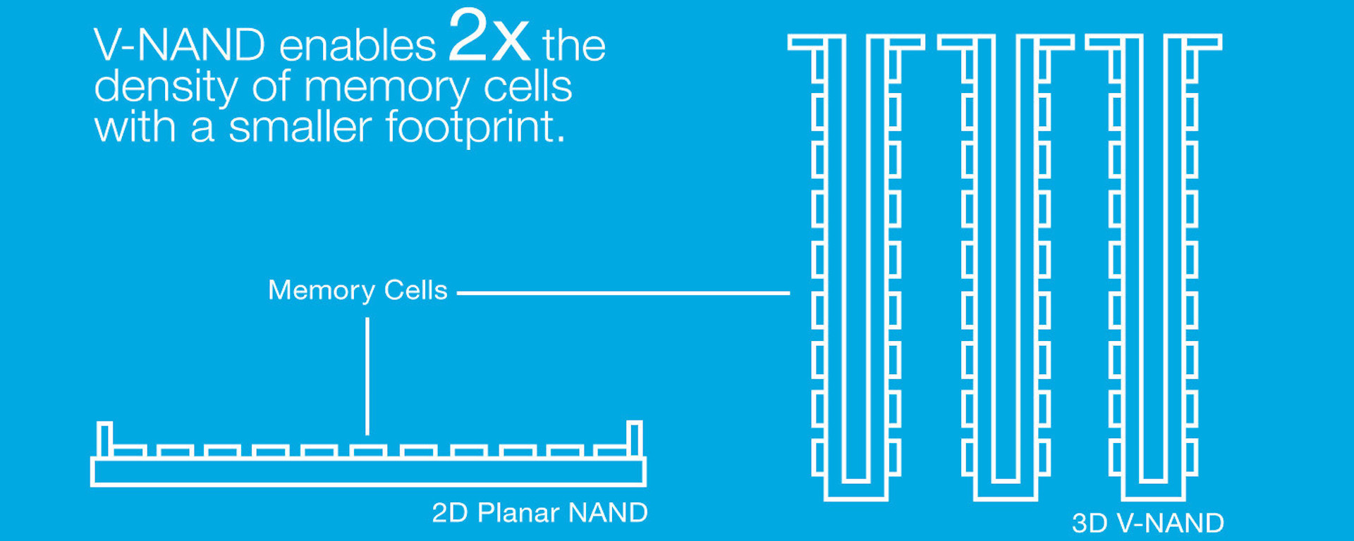
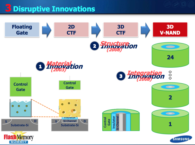
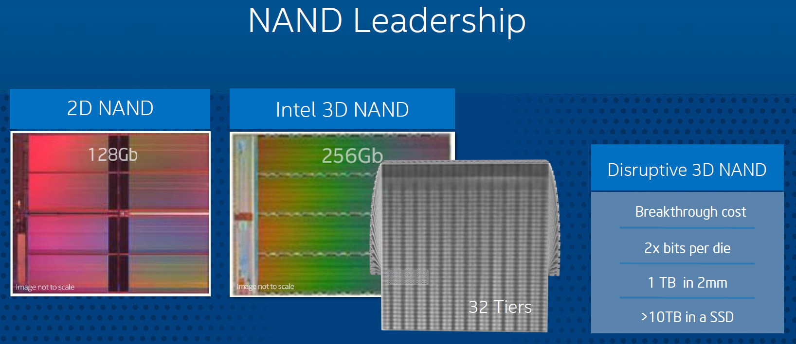
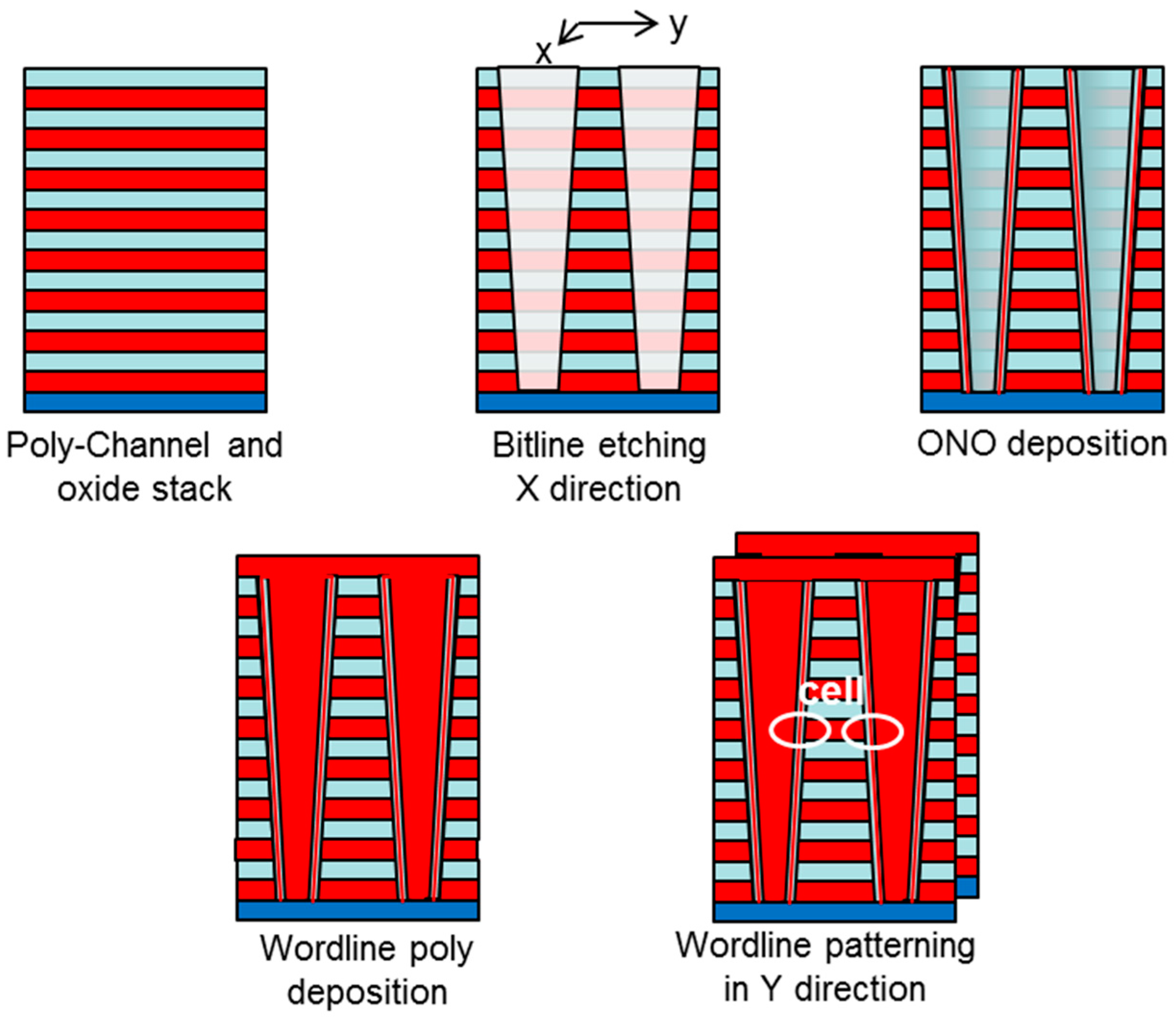
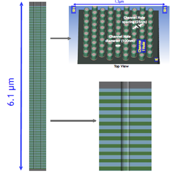
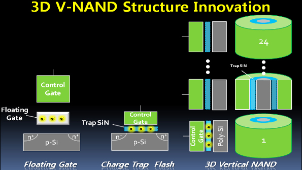
2d planar nand and 3d vertical nand the difference instead of using the conductive floating gate like all the other flash memory chips to store charge the 3d v nand technology uses silicon nitride an insulator to store charge by means of the charge trap flash ctf technology. 3d nand attempts to solve the problem of increased data storage demands in small spaces by building storage upward. Samsungs vnand technology is their version of 3d nand with some proprietory modifications in between. The way weve been explaining things youd been forgiven for thinking as most people commonly do that the v nand is the absolute same thing as a 3d nand.
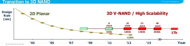
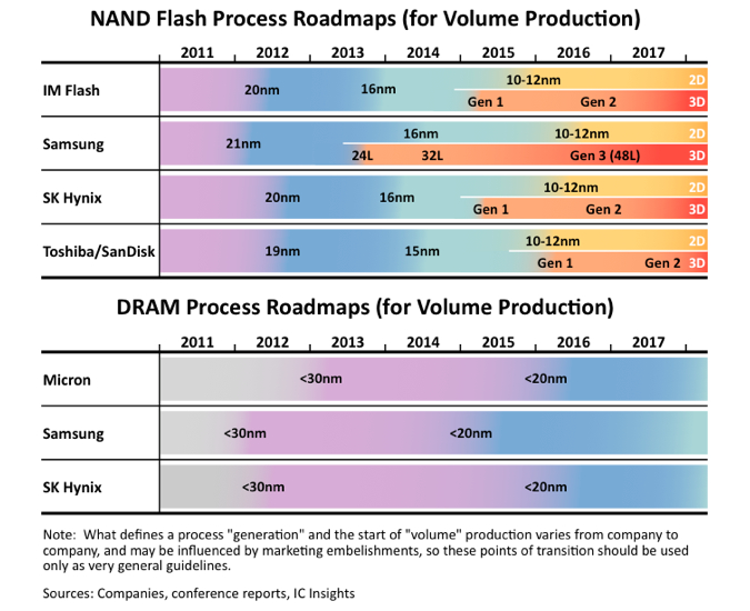
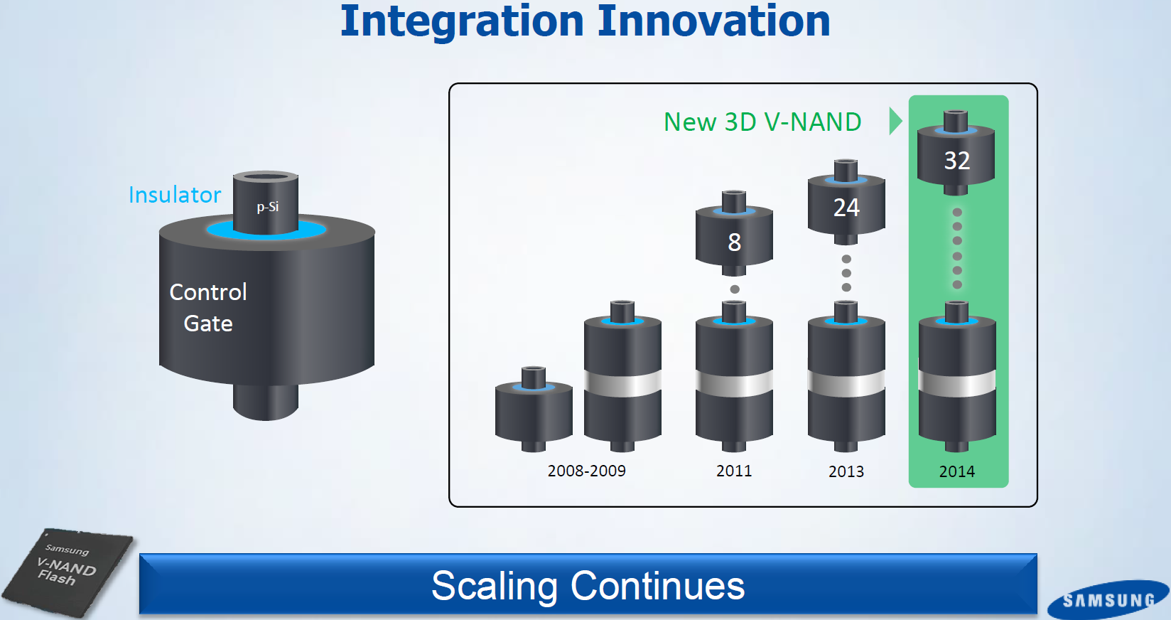
Higher density ssds basically have a higher layer count. V nand or 3d v nand is the latest technology in the flash memory world. That something was the invention of 3d v nand. An estimated density of 1tb is expected for 100 layer nand chips.
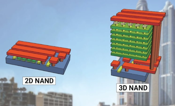
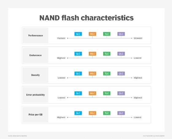
The major difference between 3d v nand and the traditional planar nand that came before is a matter of stacking. Slc mlc and tlc flash are 2d or planar.

Nand Flash Explained Mlc Vs Tlc Vnand More Gamersnexus Gaming Pc Builds Hardware Benchmarks

3d Nand How It Works Samsung Ssd 850 Pro 128gb 256gb 1tb Review Enter The 3d Era
Samsung 850 Evo 1tb 3d V Nand Ssd Review Tweaktown
The Changing Face Of Non Volatile Storage Electronic Design

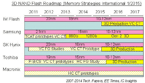
3d Nand Flash Wars Begin