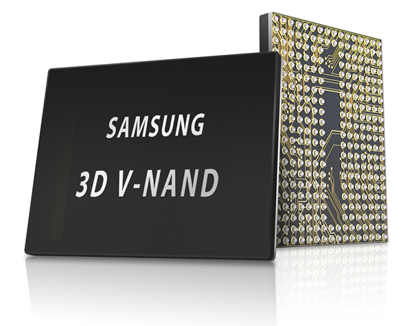
3d V Nand
In essence like the name suggests 3d v nand means an ssd made up of flash cells stacked vertically and 3 dimensionally.
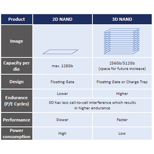
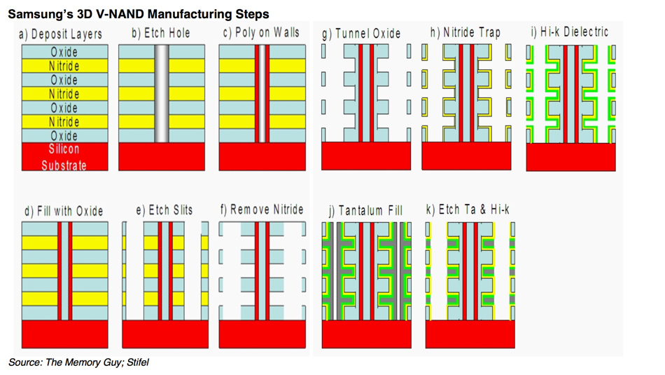
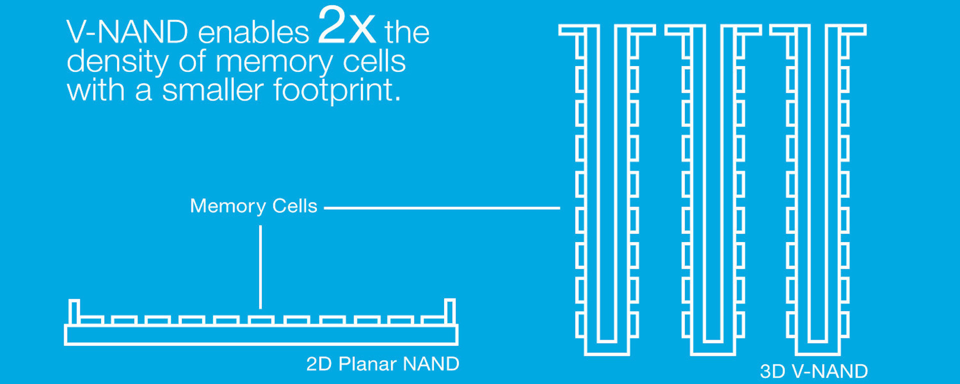
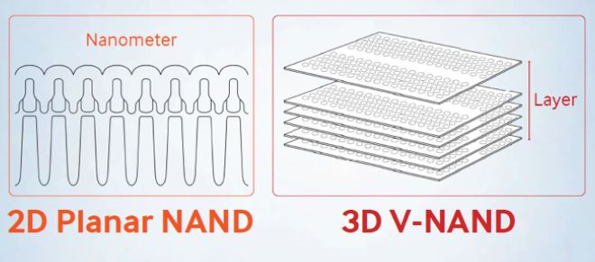
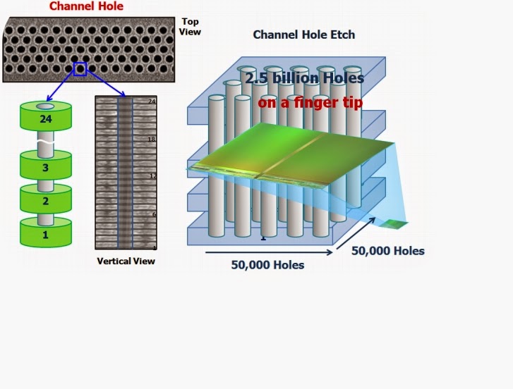
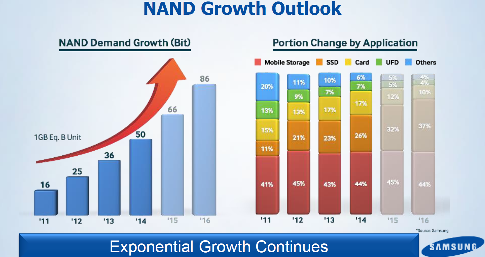
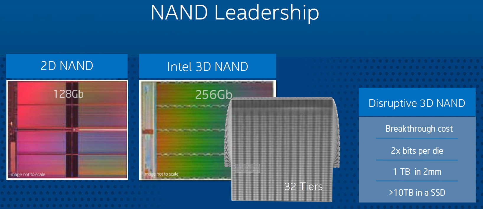
3d v nand. 3d nand is a new powerful entry into the ssd conversation. V nand discussion will follow. This is where planar nand single planes of nand cells are stacked vertically giving the v in v nand. These days up to 96 layers of cells are stacked in consumer and enterprise ssds.
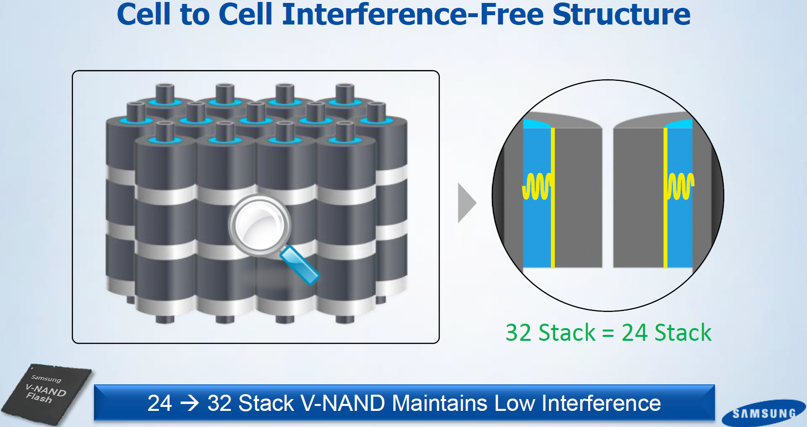
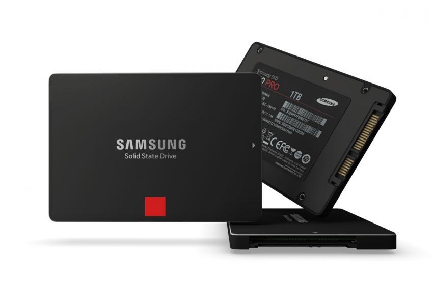
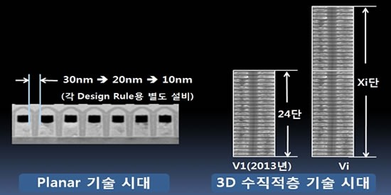
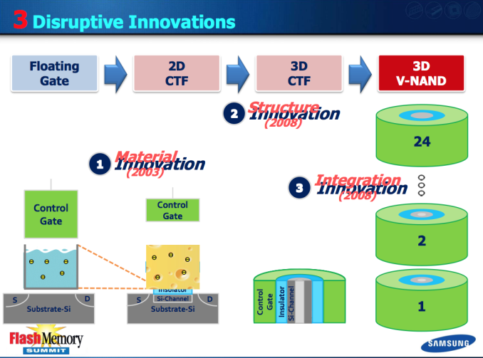
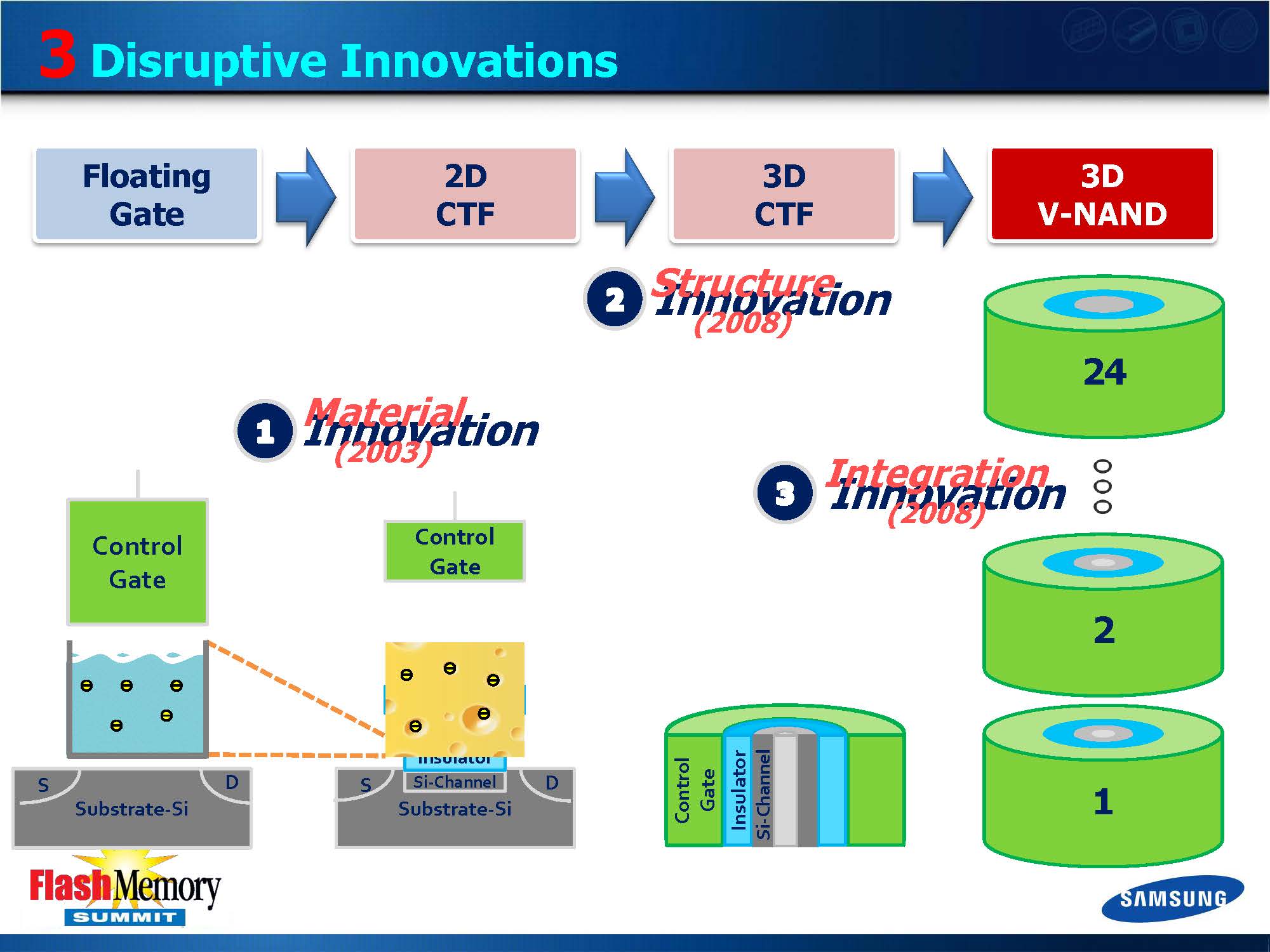
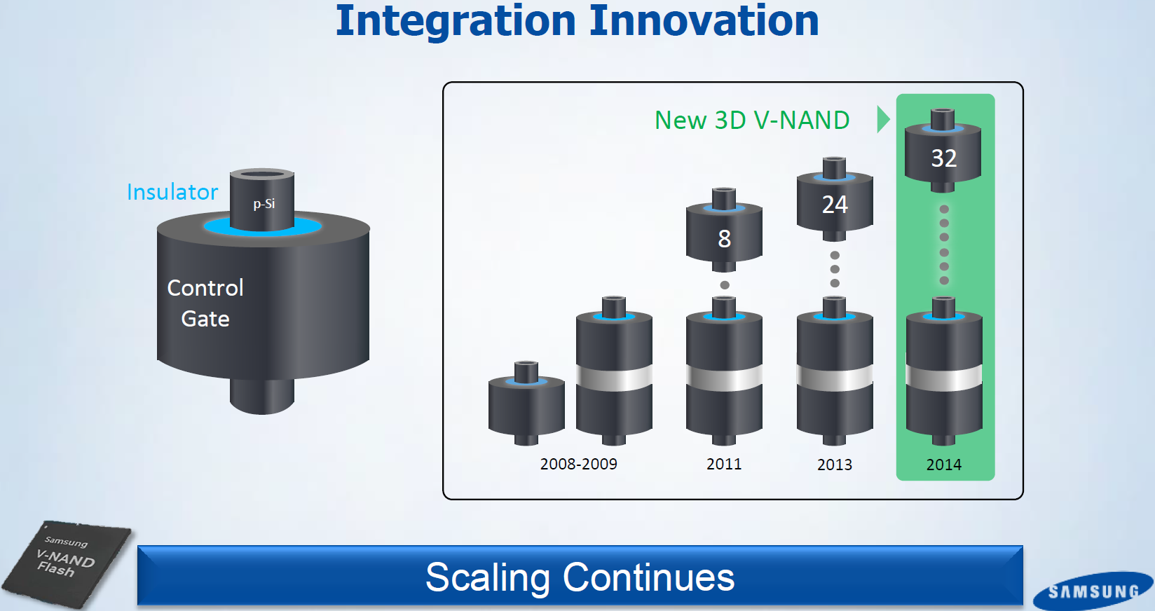
The major difference between 3d v nand and the traditional planar nand that came before is a matter of stacking. Higher density ssds basically have a higher layer count. The 3d nand specifically stacks the memorysilicon chipscells vertically on top of each other in multiple layers. Samsungs proprietary v nand technology as used in the 850 pro involves stacking 32 cell layers of cells on top of one another.
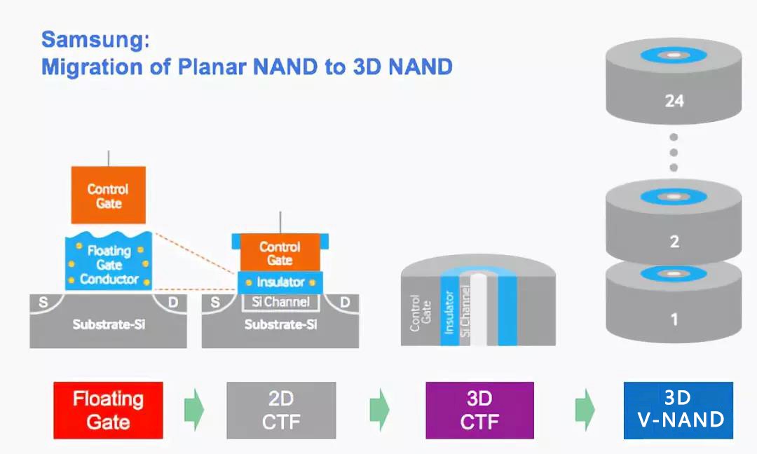
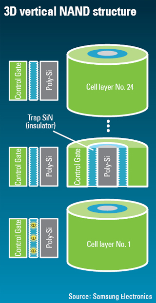
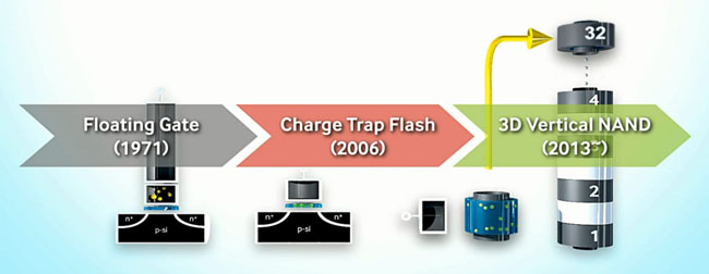
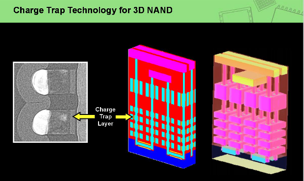
Slc mlc and tlc flash are 2d or planar. In laymans terms cheaper and faster storage and memory. In non laymans terms well lets take a look. Instead of using the conductive floating gate like all the other flash memory chips to store charge the 3d v nand technology uses silicon nitride an insulator to store charge by means of the charge trap flash ctf technology.
That something was the invention of 3d v nand. 3d nand attempts to solve the problem of increased data storage demands in small spaces by building storage upward. Hence why its called the v nand although a specific 3d nand vs. V nand or 3d v nand is the latest technology in the flash memory world.
Samsungs vnand technology is their version of 3d nand with some proprietory modifications in between. This is significant because before now most ssds have been built on 2d. The chips in question are vertically stacked in 36 48 72 or 64 and now 96 layers of flash cells. The biggest leap forward as of late has been 3d nand flash also known as vertical nand or v nand what does this mean for you.
This little modification means that there is no memory wear or flash wear caused due to short circuit currents.

Converge Network Digest Samsung S 3d V Nand Flash Memory Enters Mass Production

Samsung 3d V Nand 92 Layer Memory System Plus Consulting
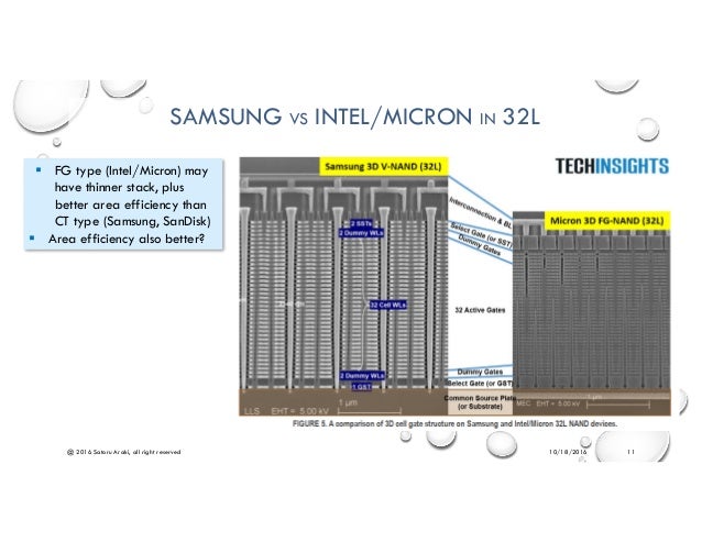
Samsung 64l 3d V Nand Techinsights
Samsung Announces Mass Production Of Industry S First 3 Bit 3d V Nand Flash Memory The Ssd Review
Hdd To 3d Nand And Beyond Oct2016 Satoruaraki